Real-time in-situ TEM observation
I use in-situ TEM to watch a-Si nanopillars etch in aqueous KOH, revealing isotropic etching and the formation and evolution of reaction-intermediate nanoclusters.
Advanced Nanoanalysis Lab
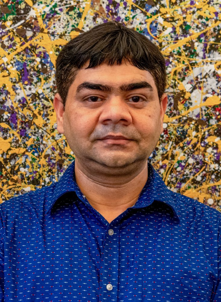
Senior Scientist · IMRE · A*STAR
Nanoscale Materials ·Electron Microscopy ·AI Image Analysis ·Lab Automation
I study materials at the nanoscale using advanced and in-situ electron microscopy to watch structures form, evolve, react, and fail. I combine AI-driven analysis, custom instrumentation, and laboratory automation to accelerate discovery and turn observations into quantitative insight.
Outside research, I enjoy learning, exploring new technologies, and turning ideas into things I can build and experiment with.
01 / Research
My work sits at the intersection of materials science, advanced microscopy, computation, and experimental automation. I use electron microscopy to observe materials processes as they happen, from nanoscale reactions and structural transformations to degradation and failure. By combining in-situ experiments with quantitative image analysis, custom instrumentation, and automated workflows, I aim to move beyond simply imaging materials to understanding how and why they evolve.
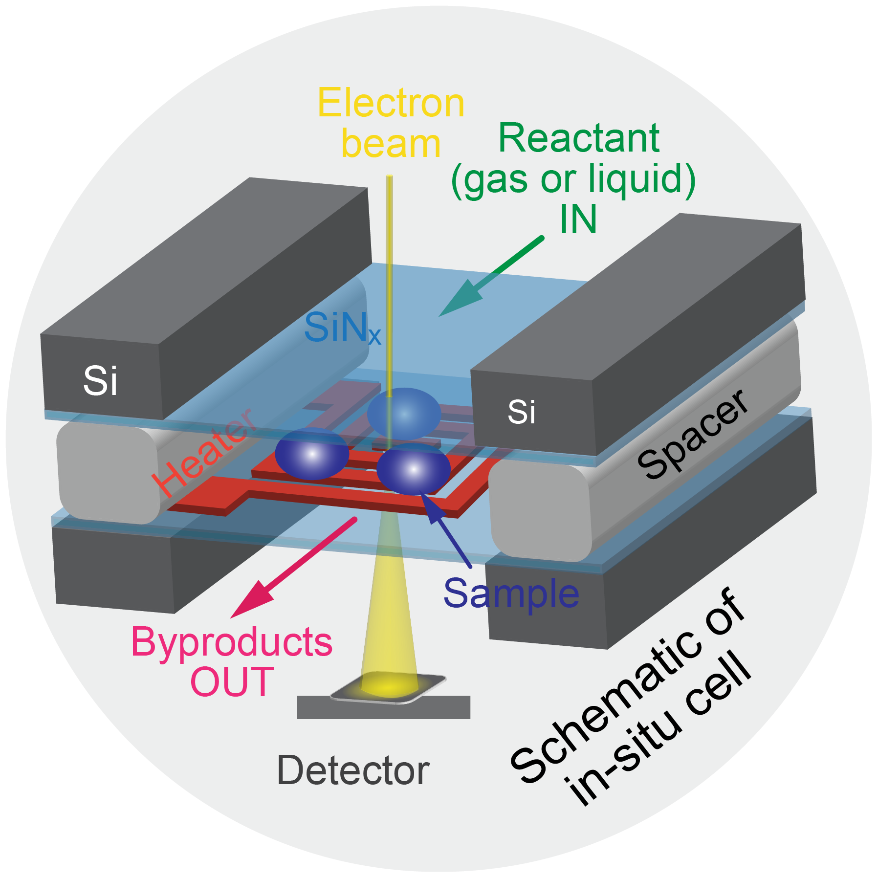
01 Real-Time Observation
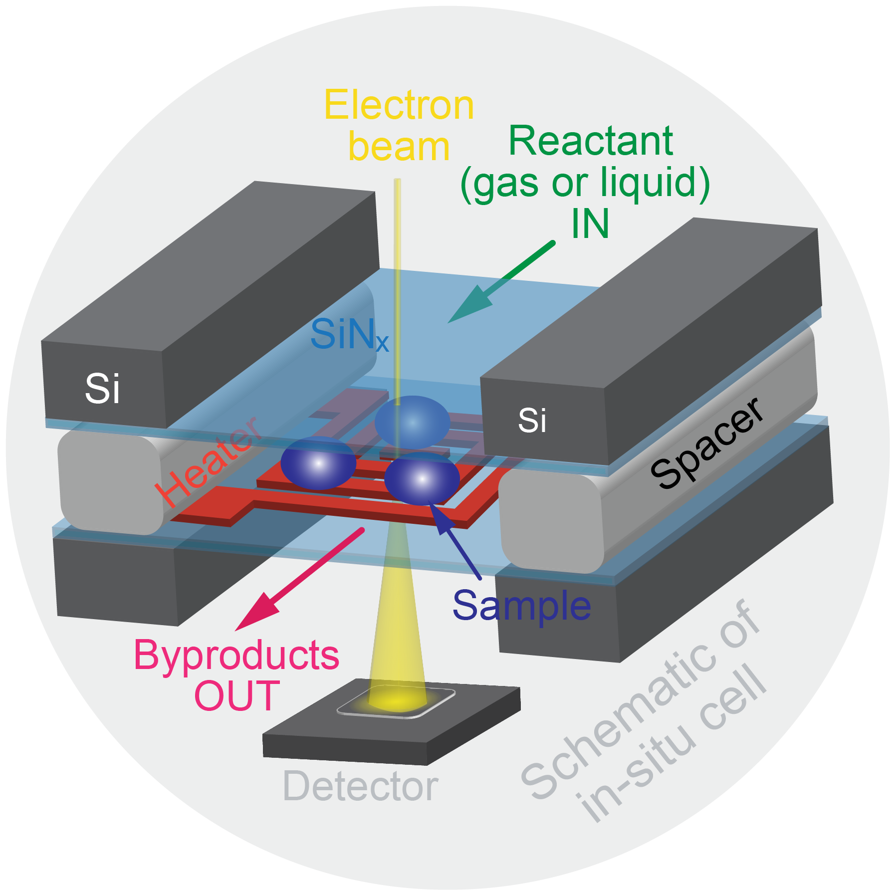
I use in-situ TEM to watch a-Si nanopillars etch in aqueous KOH, revealing isotropic etching and the formation and evolution of reaction-intermediate nanoclusters.
02 Interfacial Phenomena
I use in-situ TEM to visualize water vapour in dense a-Si nanopillar arrays, revealing capillary condensation and liquid bridge formation.
03 Quantitative Analysis
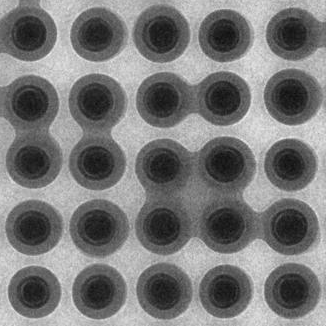
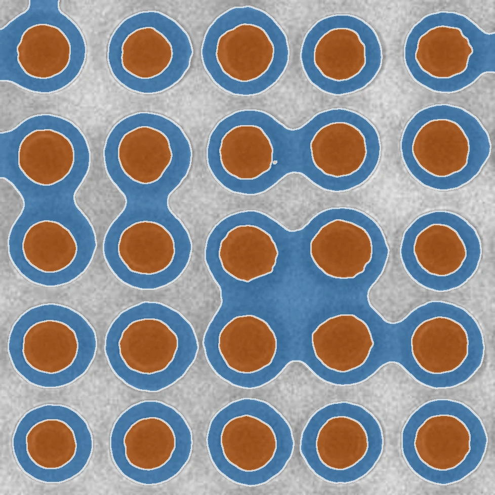 TEM imageAI segmentation
 AI-based segmentation identifies the nanopillars and condensed water, converting complex microscopy images into quantitative data for tracking their evolution.
04 Experimental Engineering

I design custom TEM holders for liquid-phase experiments, enabling controlled wetting, drying, and etching studies directly inside the microscope.
02 / Research highlights
P01
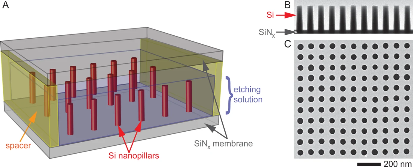
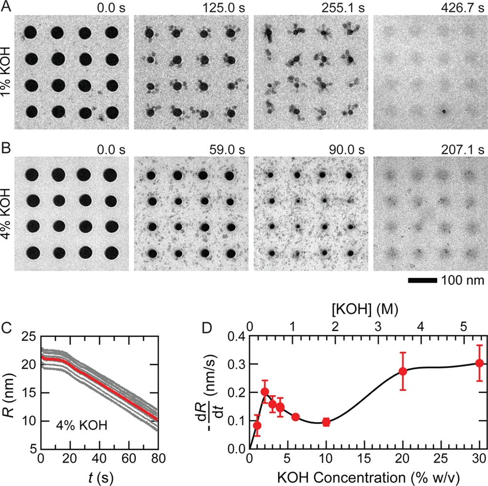
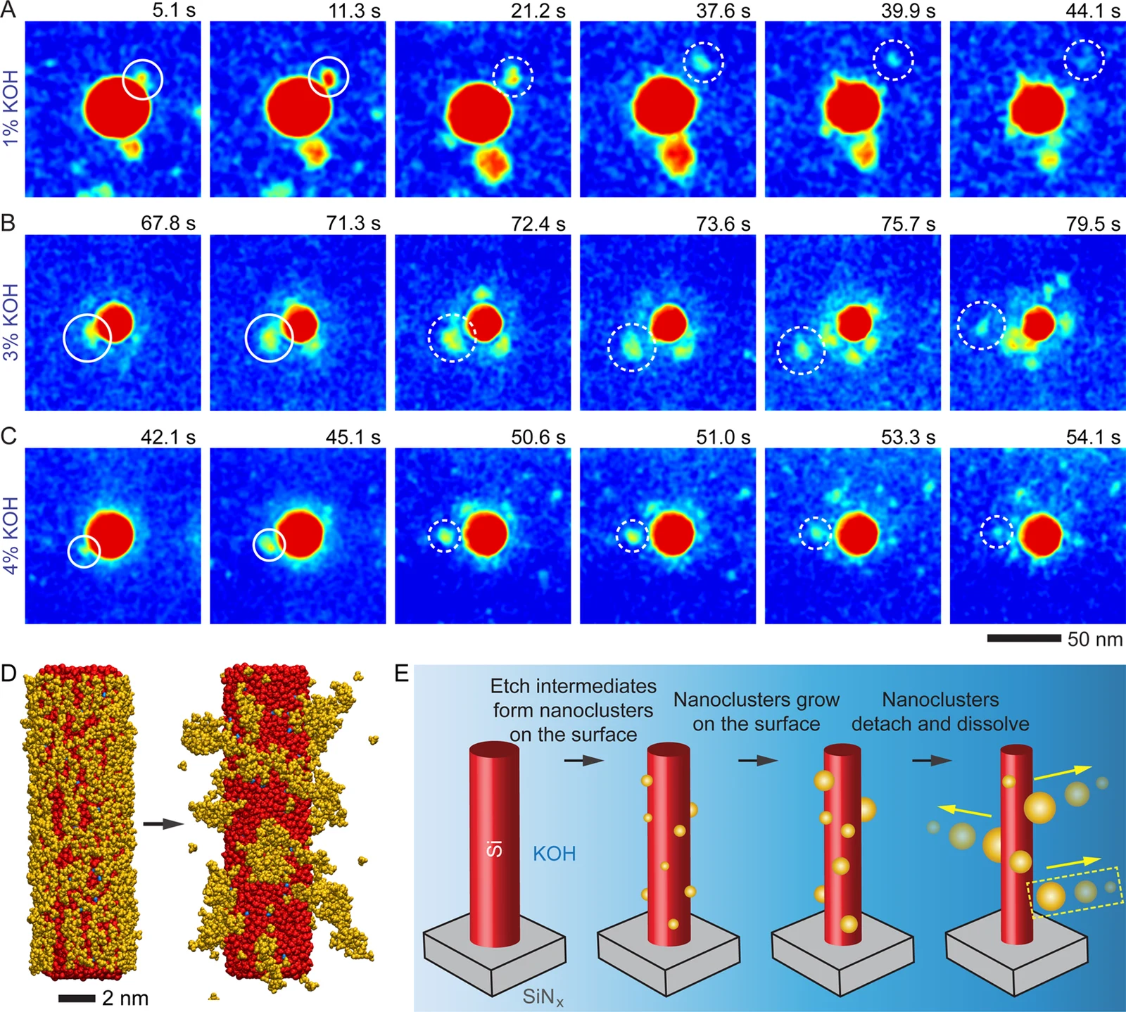
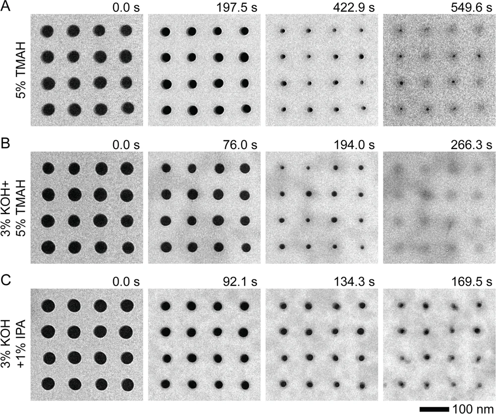
Wet chemical etching is a key process in fabricating silicon (Si) nanostructures. Currently, wet etching of Si is proposed to occur through the reaction of surface Si atoms with etchant molecules, forming etch intermediates that dissolve directly into the bulk etchant solution. Here, using in situ transmission electron microscopy (TEM), we follow the nanoscale wet etch dynamics of amorphous Si (a-Si) nanopillars in real-time and show that intermediates generated during alkaline wet etching first aggregate as nanoclusters on the Si surface and then detach from the surface before dissolving in the etchant solution. Molecular dynamics simulations reveal that the molecules of etch intermediates remain weakly bound to the hydroxylated Si surface during the etching and aggregate into nanoclusters via surface diffusion instead of directly diffusing into the etchant solution. We confirmed this model experimentally by suppressing the formation of nanoclusters of etch intermediates on the Si surfaces by shielding the hydroxylated Si sites with large ions. These results suggest that the interaction of etch intermediates with etching surfaces controls the solubility of reaction intermediates and is an important parameter in fabricating densely packed clean 3D nanostructures for future generation microelectronics.
Reprinted with permission from Aabdin et al., Nano Lett. 2017. © 2017 American Chemical Society
P02
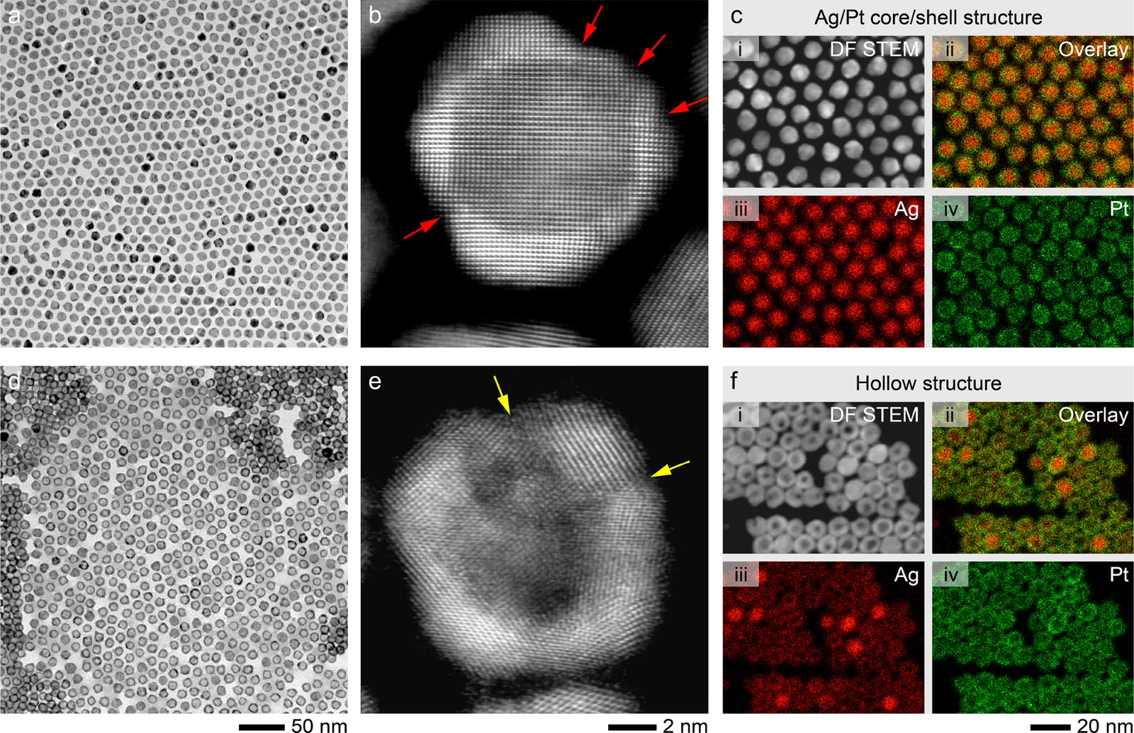
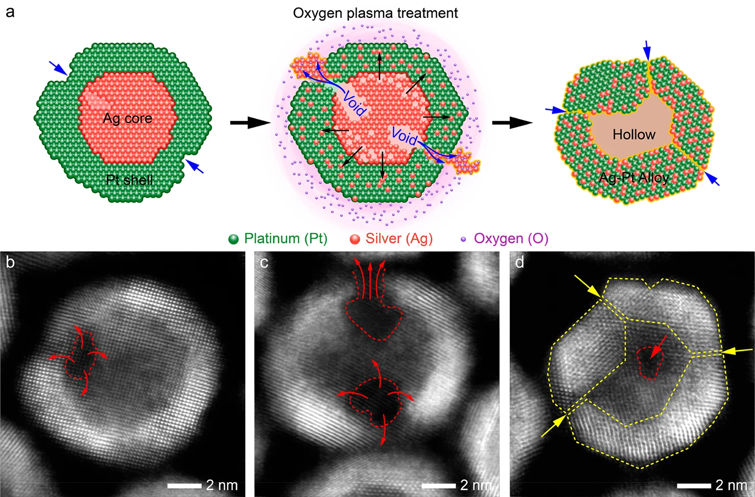
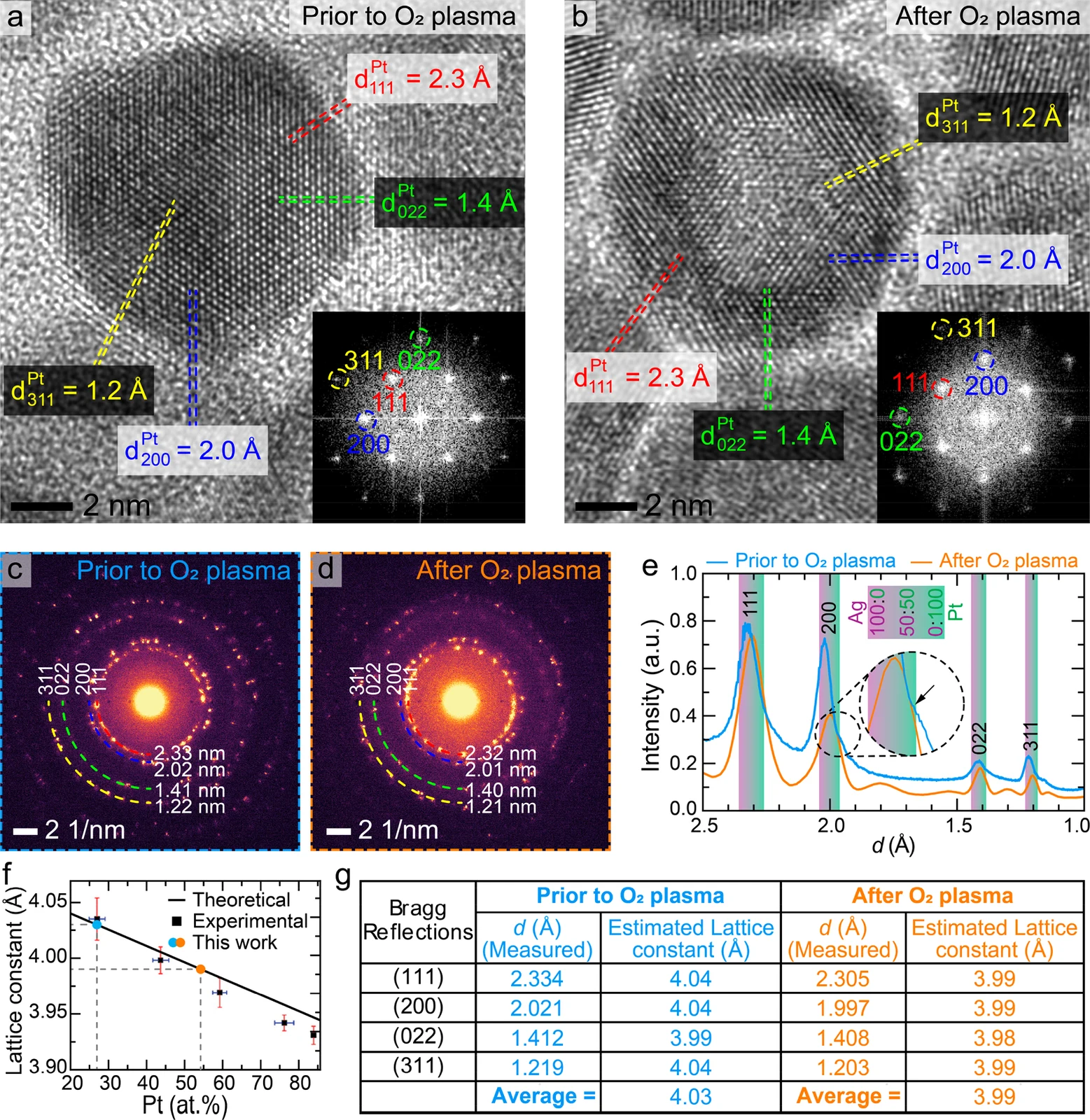
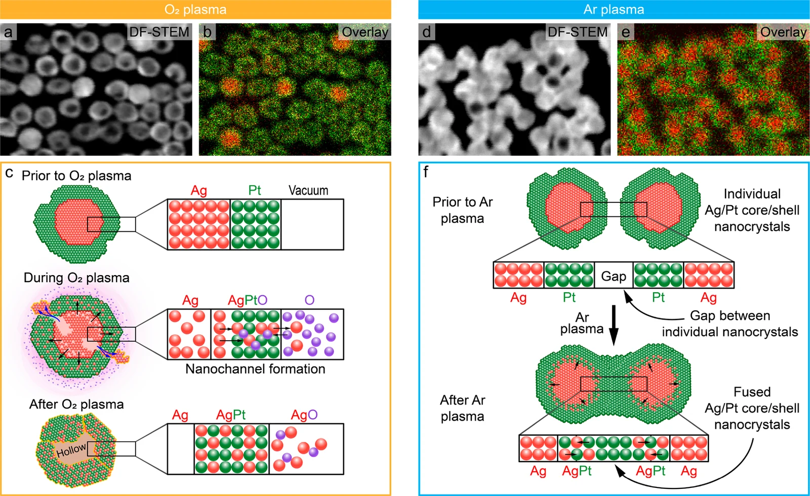
Platinum-based metal catalysts are considered excellent converters in various catalytic reactions, particularly in fuel cell applications. The atomic structure at the nanocrystal surface and the metal interface both influence the catalytic performance, controlling the efficiency of the electrochemical reactions. Here we report the synthesis of Ag/Pt and Ag/Pd core/shell nanocrystals and insight into the formation mechanism of these bimetallic core/shell nanocrystals when undergoing oxygen plasma treatment. We carefully designed the oxidation treatment that determines the structural and compositional evolution. The accelerated oxidation-triggered diffusion of Ag toward the outer metal shell leads to the Kirkendall effect. After prolonged oxygen plasma treatment, most core/shell nanocrystals evolve into hollow spheres. At the same time, a minor fraction of the metal remains unchanged with a well-protected Ag core and a monocrystalline Pt or Pd shell. We hypothesize that the O2 plasma disturbs the Pt or Pd shell surface and introduces active O species that react with the diffused Ag from the inside out. Based on EDX elemental mapping, combined with several electron microscopic techniques, we deduced the formation mechanism of the hollow structures to be as follows: (I) the oxidation of Ag within the Pt or Pd lattice causes a disrupted crystal lattice of Pt or Pd; (II) nanochannels arise at the defect locations on the Pt or Pd shell; (III) the remaining Ag atoms pass through these nanochannels and leave a hollow crystal behind. Our findings deepen the understanding of interface dynamics of bimetallic nanostructured catalysts under an oxidative environment and unveil an alternative approach for catalyst pretreatment.
Reprinted with permission from Wu et al., ACS Nano 2023. © 2023 American Chemical Society
P03
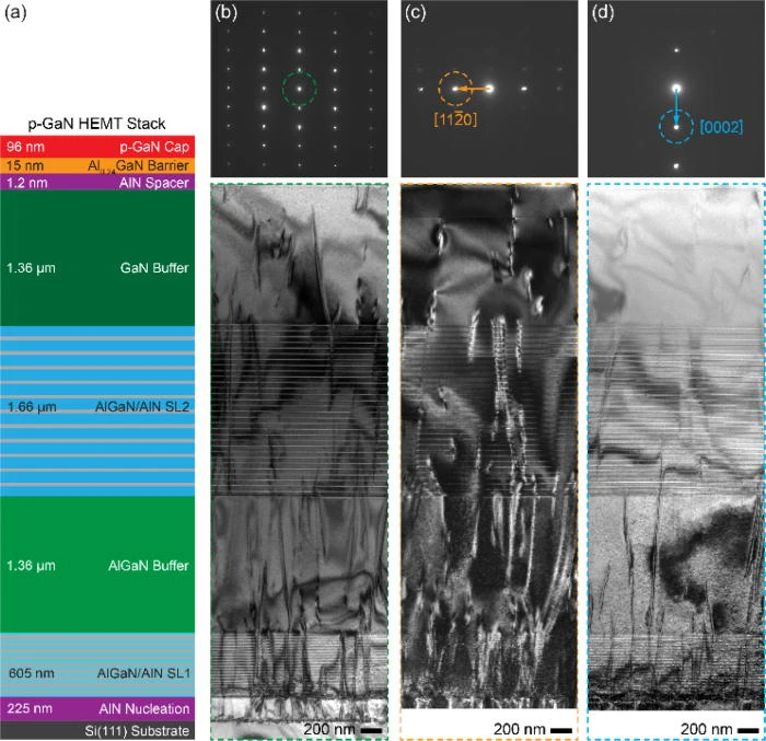
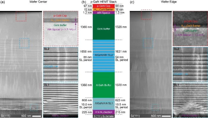
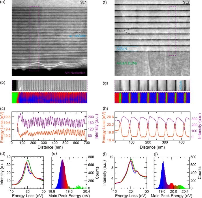
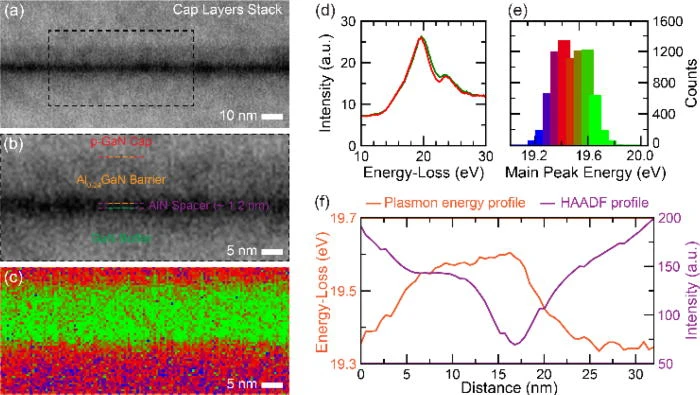
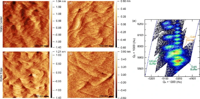
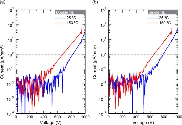
Realization of high crystal quality GaN layers on silicon substrates requires a great control over epitaxy as well as detailed characterization of the buried defects and propagating dislocations within the epilayers. In this Letter, we present the microstructural characterization of AlxGa1−xN/GaN high electron mobility transistor (HEMT) structures epitaxially grown on 200 mm Si (111) substrates with superlattice (SL) buffers. The HEMT stack is also composed of an intermediate thick AlxGa1−xN layer sandwiched between the short-period and long-period AlxGa1−xN/AlN SLs. Structural and morphological characteristics of the GaN-based epilayers are studied to assess the quality of the HEMT stack grown on such 200 mm diameter substrates. The detailed microstructural uniformity of the epilayers is addressed by the transmission electron microscopy (TEM) technique. In depth scanning TEM with electron energy loss spectroscopy (EELS) investigations have been carried out to probe the microstructural quality of the HEMT stack comprising of such short- and long-period AlxGa1−xN/AlN SLs. The EELS-plasmon maps are utilized to address the sharp interface characteristics of the SL layers as well as the top active p-GaN/AlxGa1−xN/GaN layers. This work highlights the capability of high-resolution TEM as a complementing characterization method to produce reliable AlxGa1−xN/GaN HEMTs on such a large diameter silicon substrate.
Reproduced from Aabdin et al., Applied Physics Letters 2023, with the permission of AIP Publishing
P04
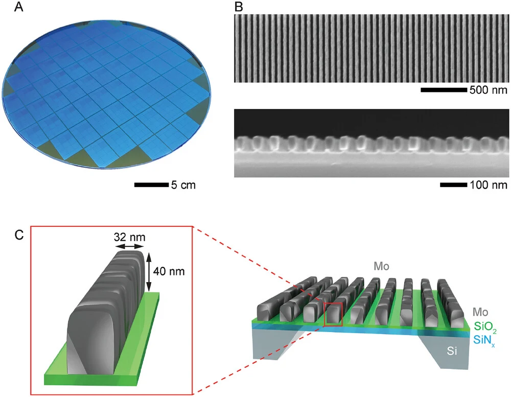
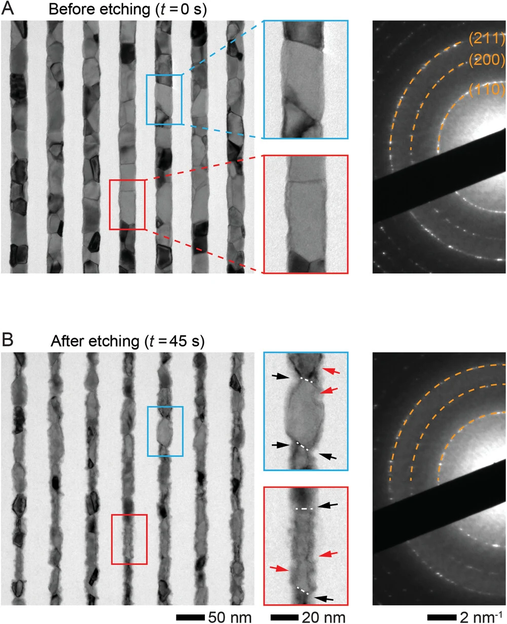
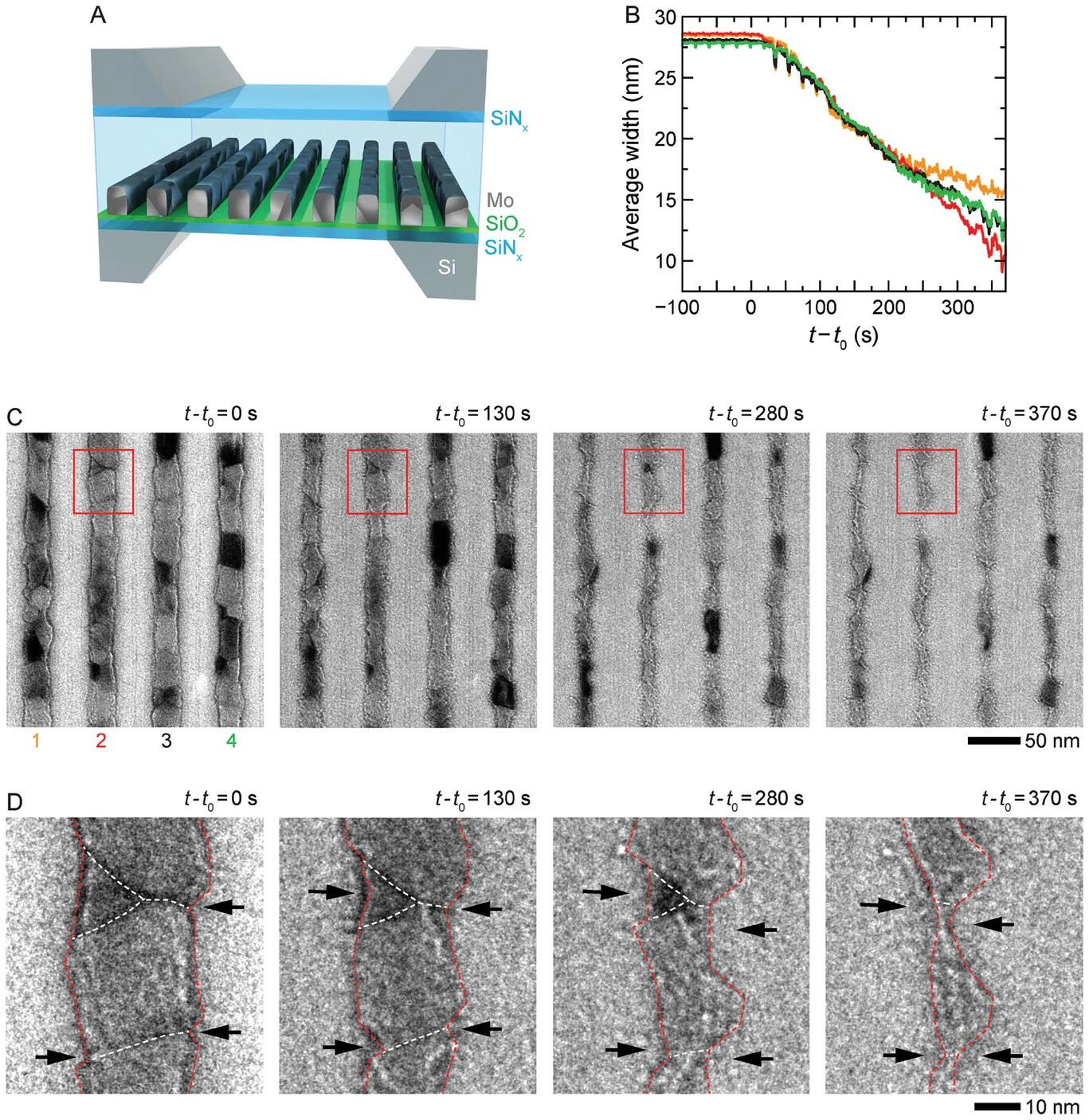
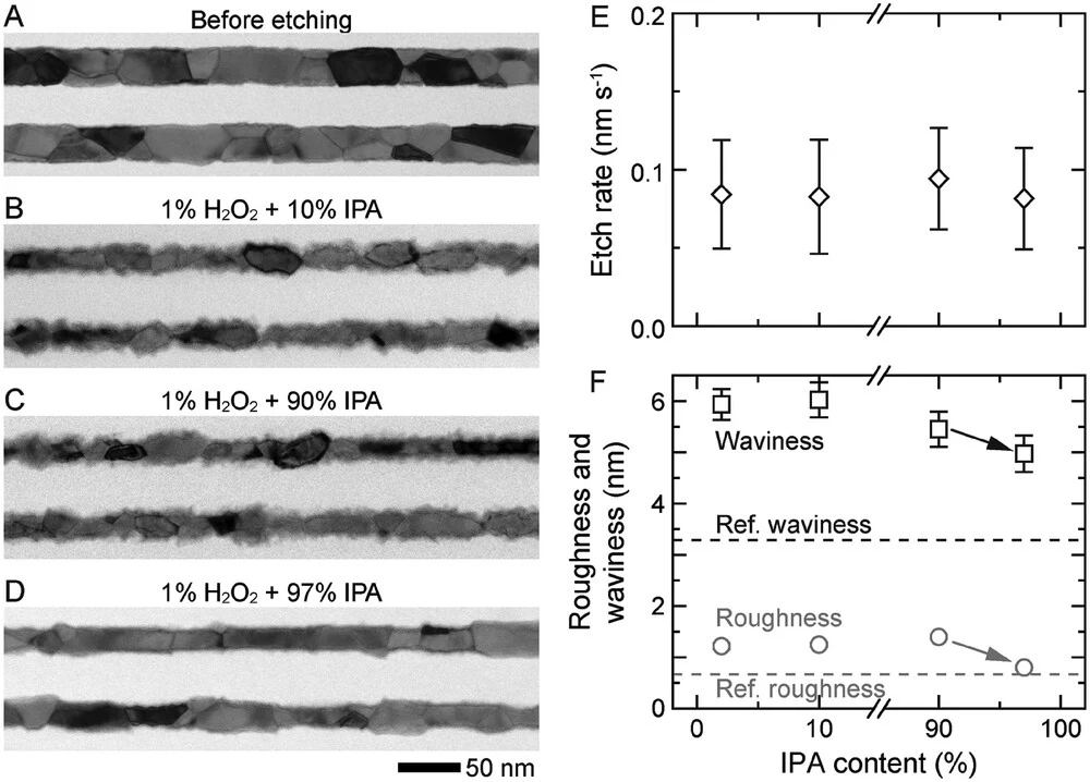
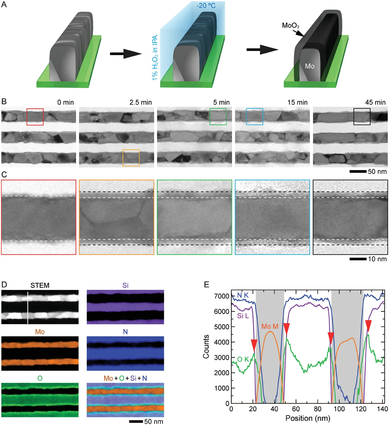
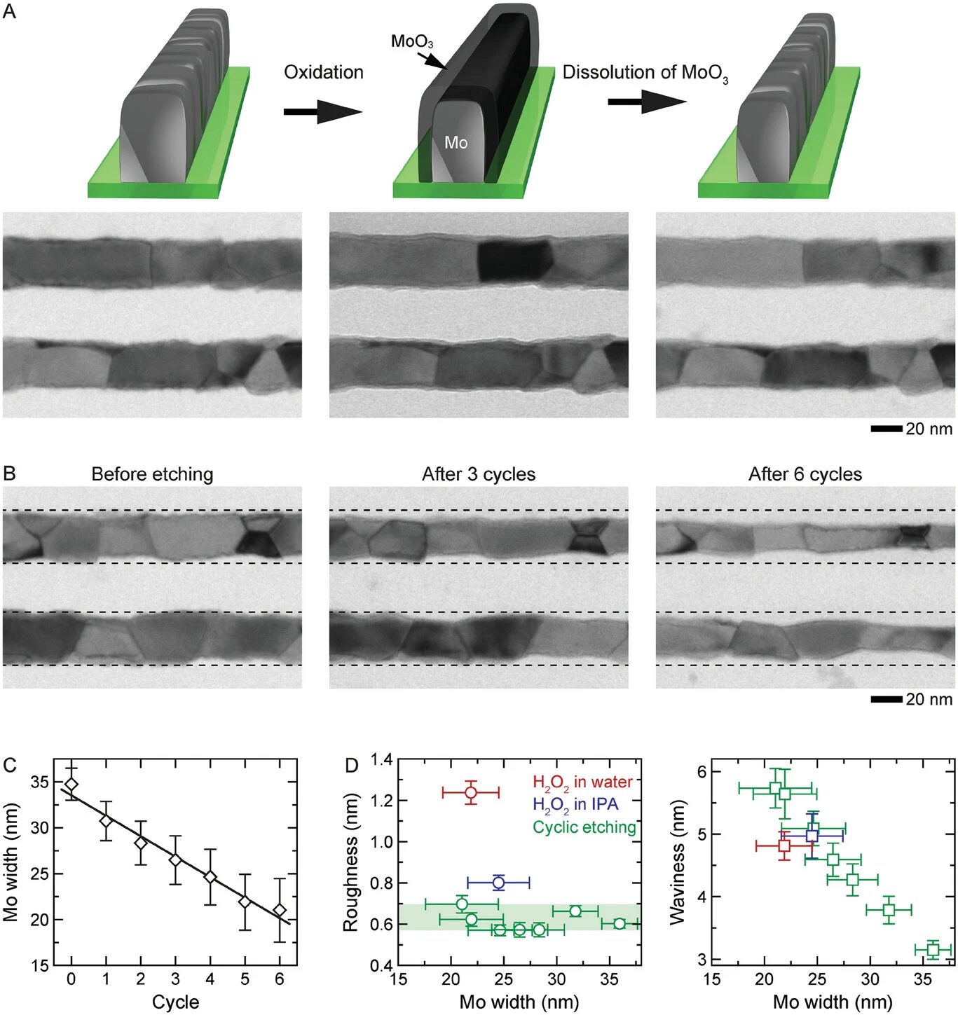
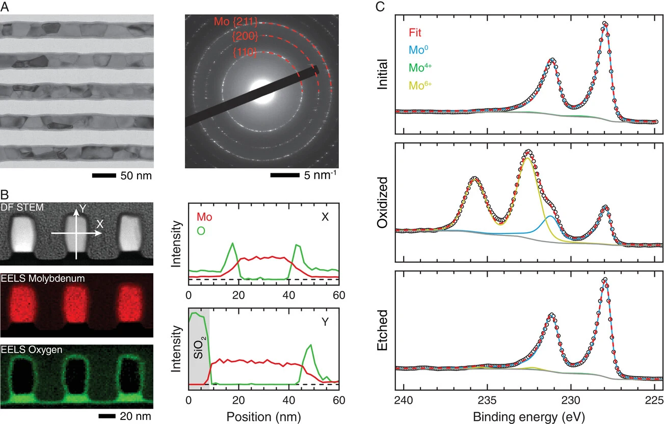
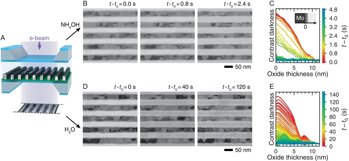
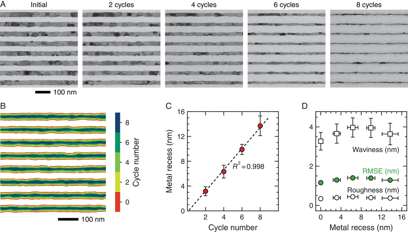
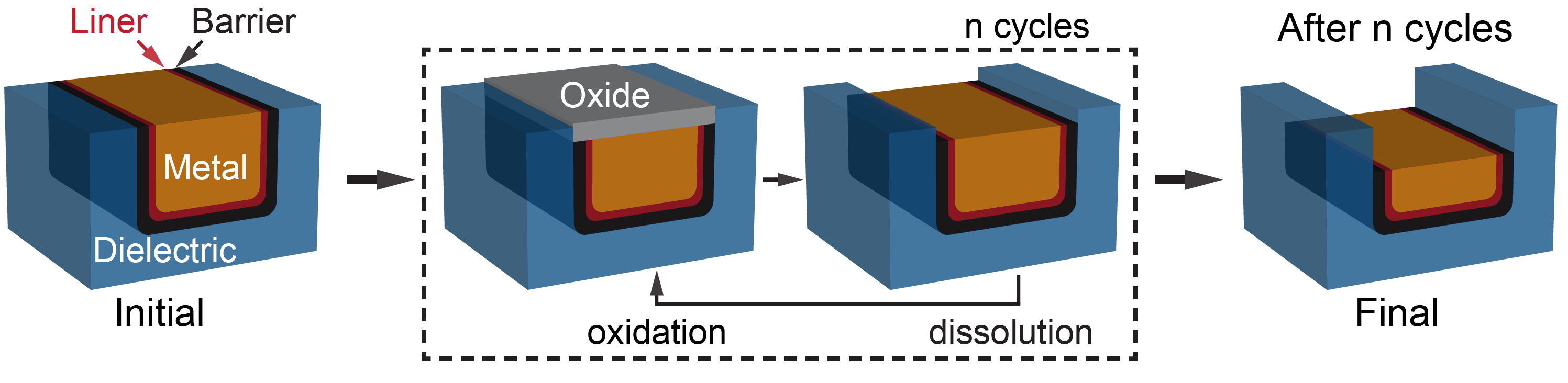
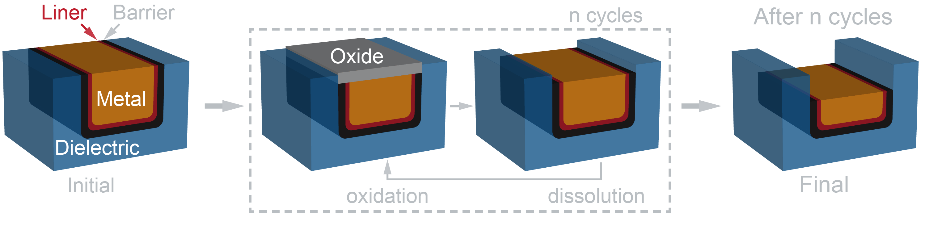
With the persistent downscaling of integrated circuits, molybdenum (Mo) is currently considered a potential replacement for copper (Cu) as a material for metal interconnects. However, fabricating metal nanostructures with critical dimensions of the order of 10 nm and below is challenging. This is because the very high density of grain boundaries (GBs) results in highly non-uniform surface profiles during direct wet etching. Moreover, wet etching of Mo with conventional aqueous solutions is problematic, as products of Mo oxidation have different solubility in water, which leads to increased surface roughness. Here, a process is shown for achieving a stable and uniform soluble surface layer of Mo oxide by wet oxidation with H2O2 dissolved in IPA at −20 °C. The oxide layer is then selectively dissolved, and by repeating the oxidation and dissolution multiple times, a uniform etch profile is demonstrated with a fine control over the metal recess. Ultimately, this presents a method of precise and uniform wet etching for Mo and other metals needed to fabricate complex nanostructures that are critical in developing next-generation electronic devices.
Figures and video: Saidov et al., Adv. Funct. Mater. 2024, CC BY 4.0
P05
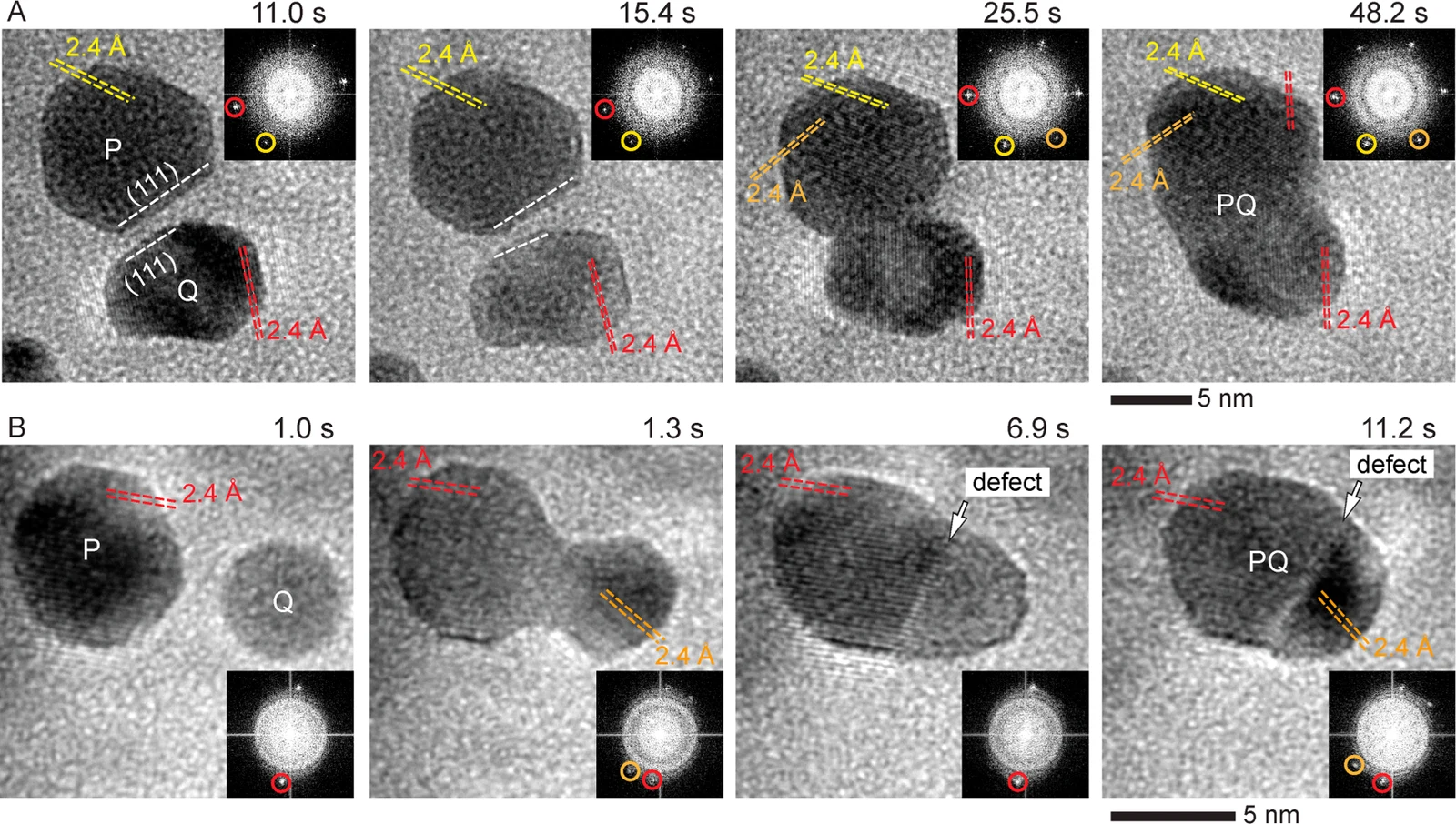
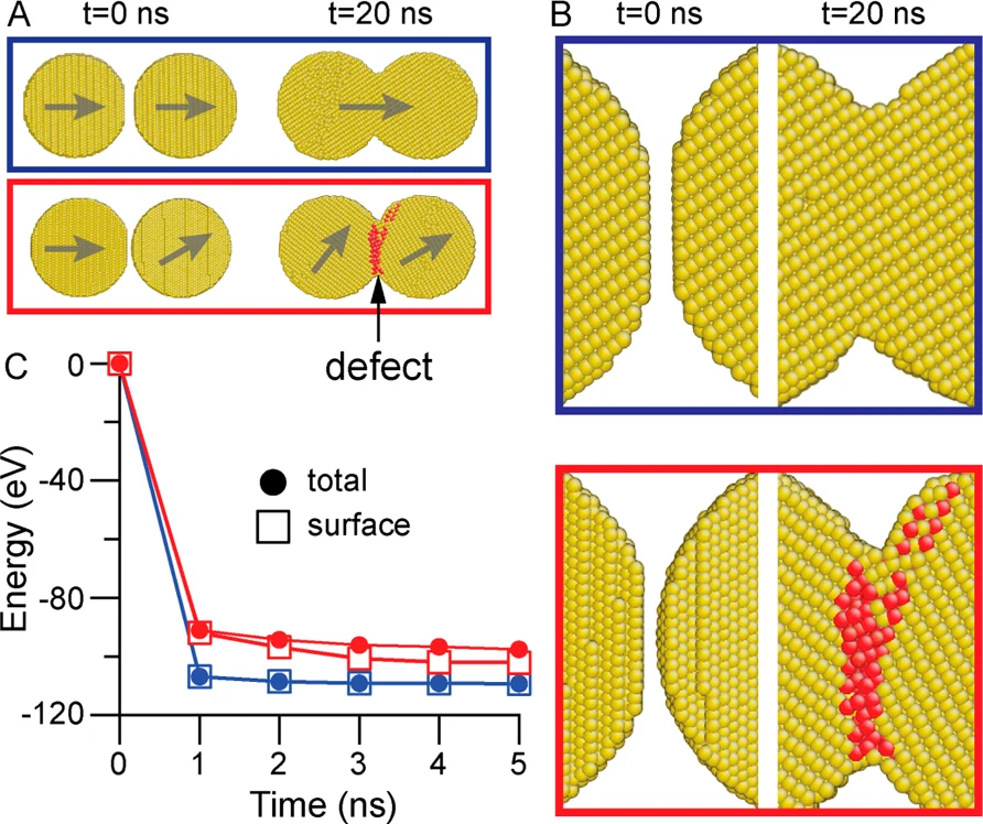
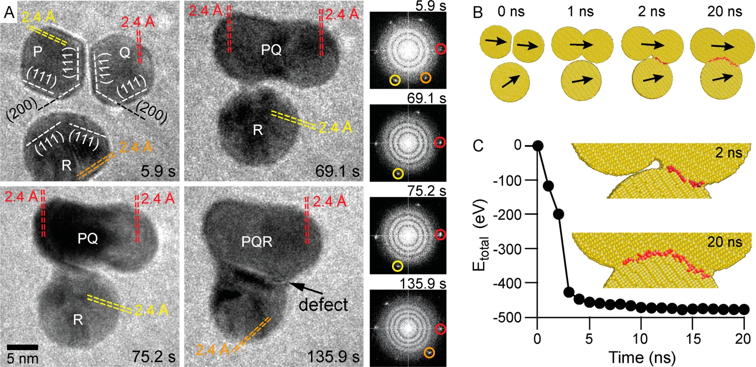
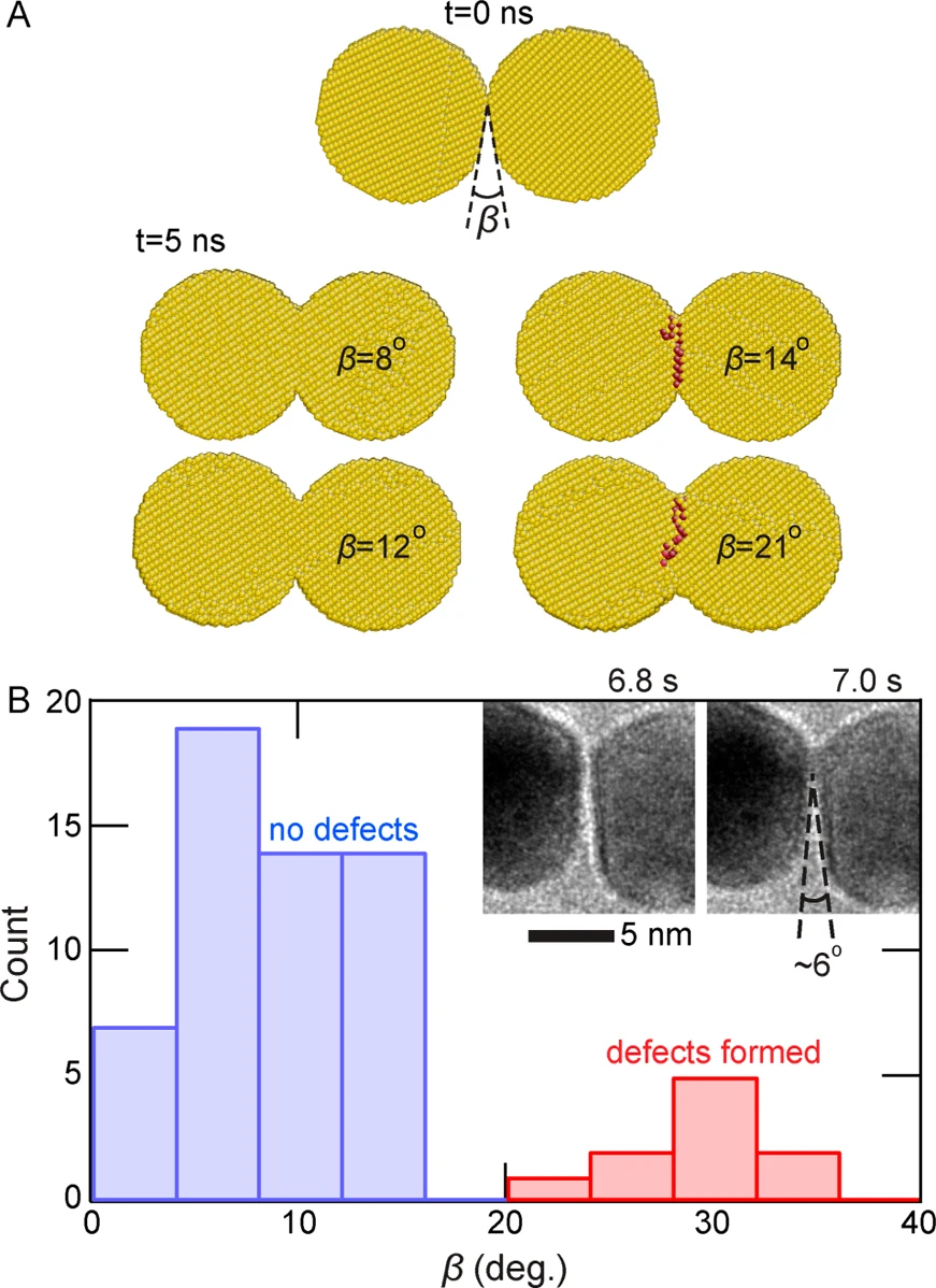
Nanocrystal bonding is an important phenomenon in crystal growth and nanoscale welding. Here, we show that for gold nanocrystals bonding in solution can follow two distinct pathways: (1) coherent, defect-free bonding occurs when two nanocrystals attach with their lattices aligned to within a critical angle; and (2) beyond this critical angle, defects form at the interfaces where the nanocrystals merge. The critical misalignment angle for ∼10 nm crystals is ∼15° in both in situ experiments and full-atom molecular dynamics simulations. Understanding the origin of this critical angle during bonding may help us predict and manage strain profiles in nanoscale assemblies and inspire techniques toward reproducible and extensible architectures using only basic crystalline blocks.
Reprinted with permission from Aabdin et al., Nano Lett. 2014, 14, 6639. © 2014 American Chemical Society
P06
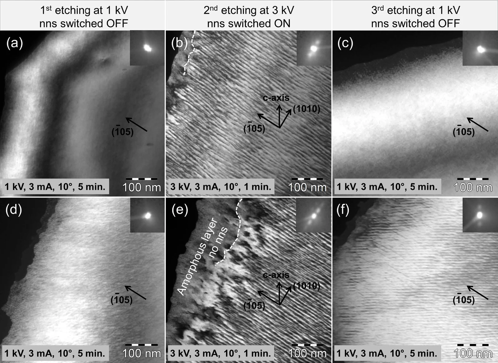
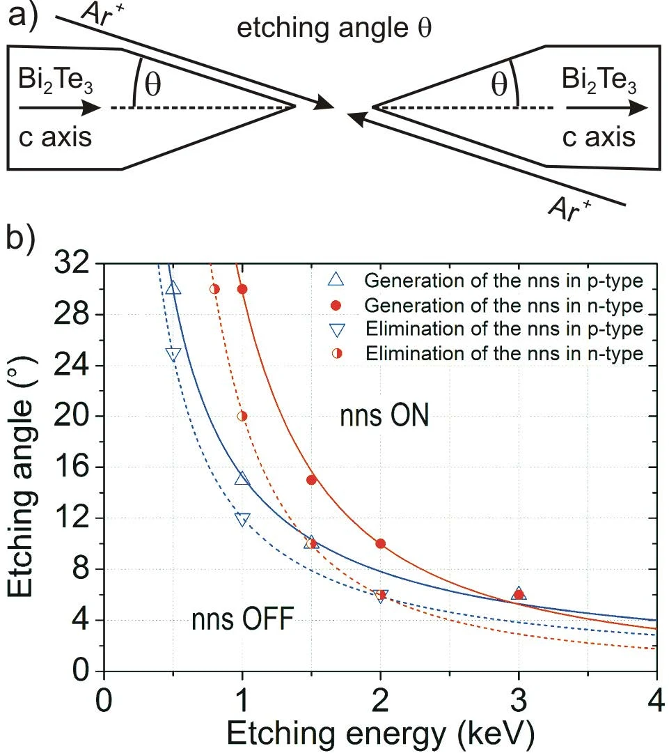
In Bi2Te3 materials the natural nanostructure (nns) with a wavelength of 10 nm can be reproducibly switched ON and OFF by Ar+ ion irradiation at 1.5 and 1 keV. Controlled formation of the nns in Bi2Te3 materials has potential for reducing its thermal conductivity and could increase the thermoelectric figure of merit.
Author's own figures (thesis version); final version published in Aabdin et al., Adv. Mater. 2012, 24, 4605
P07
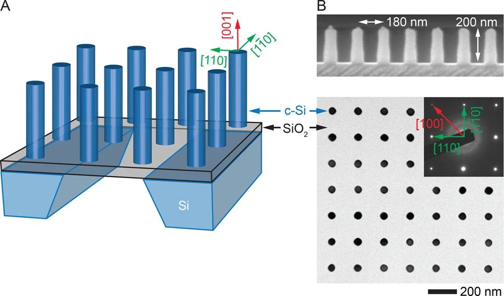
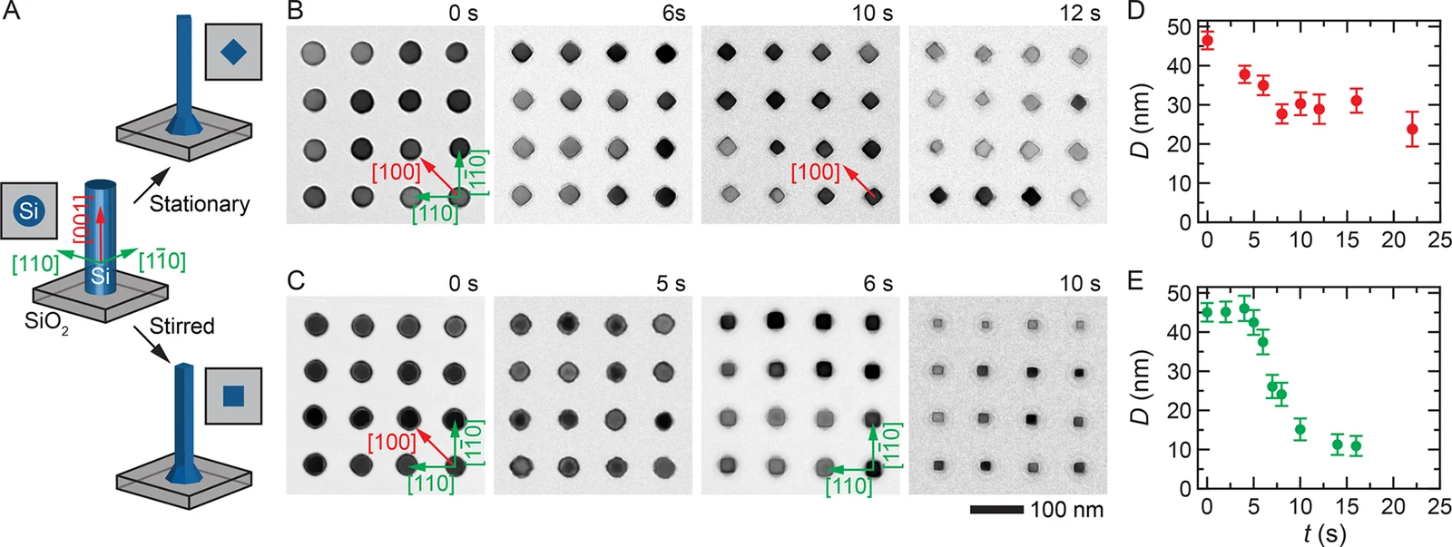
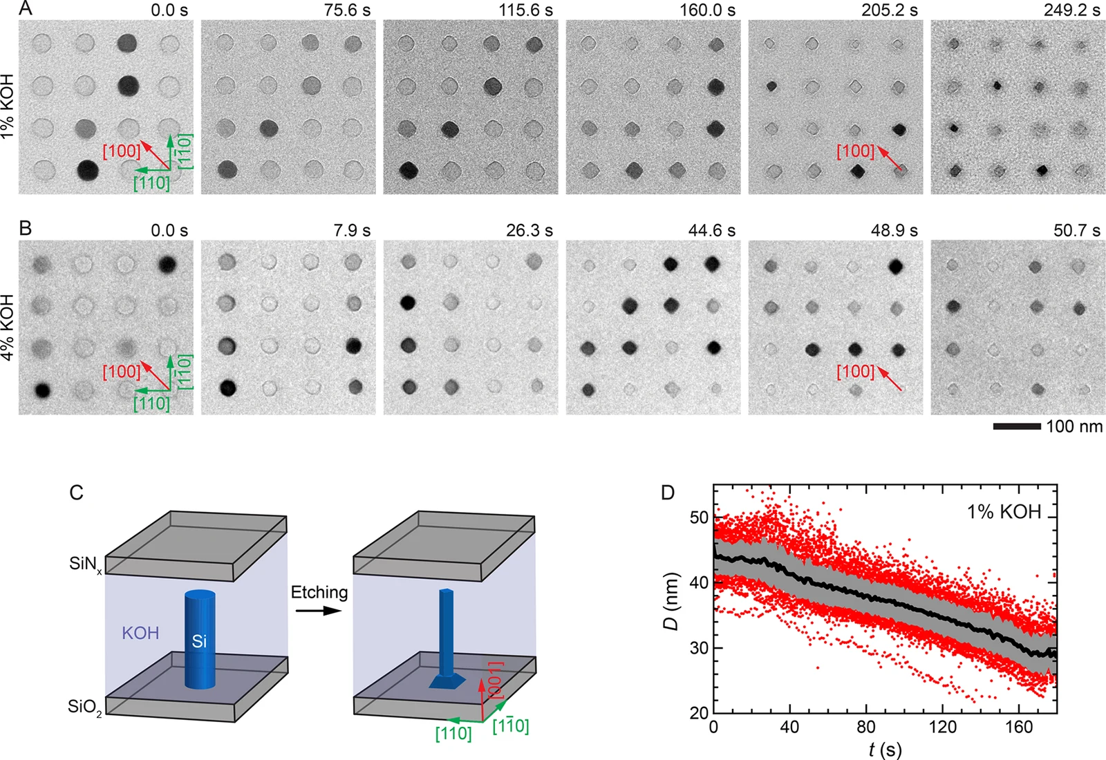
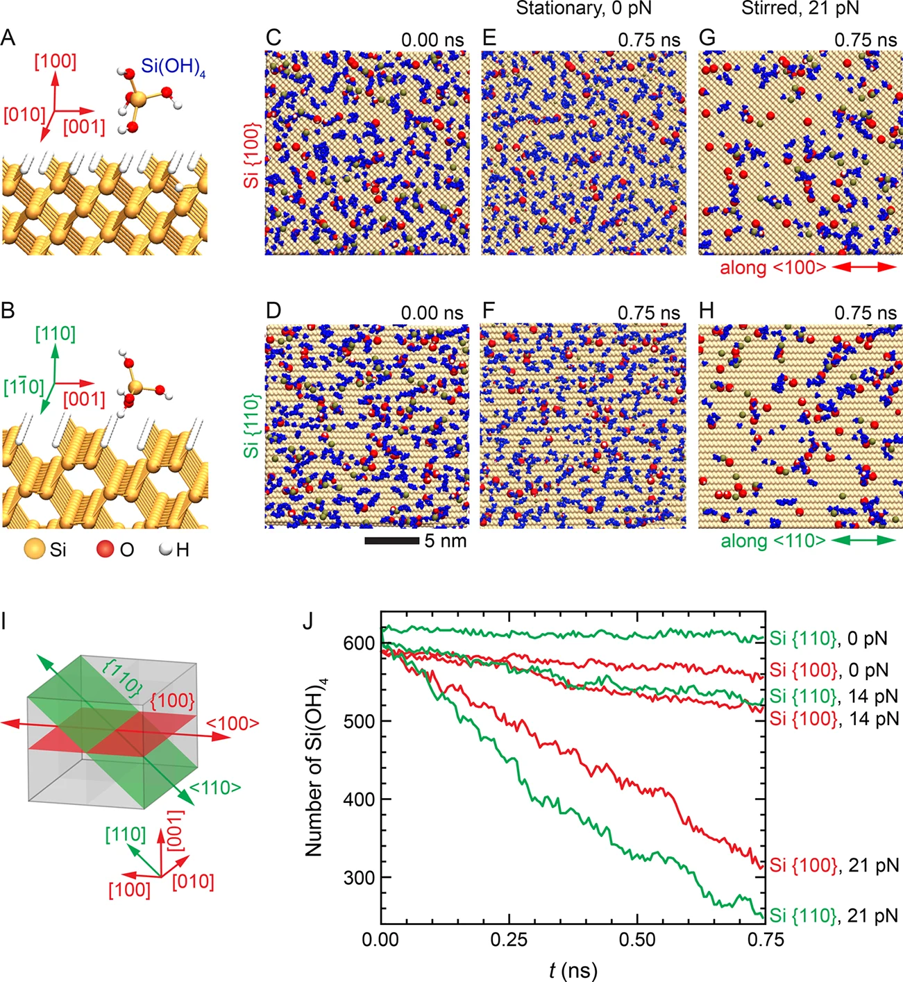
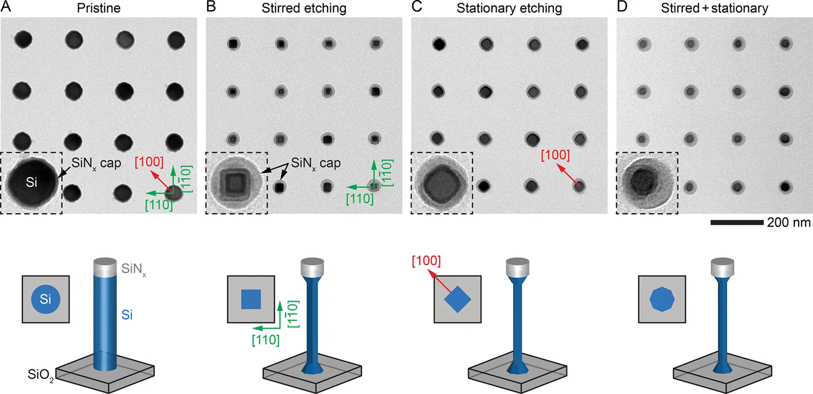
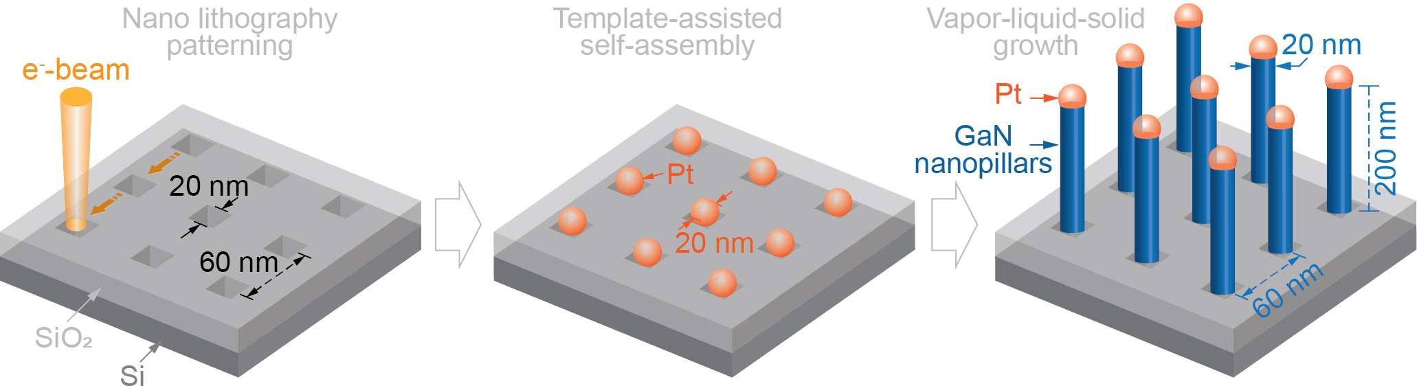
Anisotropic wet etching of crystalline silicon (c-Si) is a key chemical process used in microelectronic device fabrication. Controlled fabrication of c-Si nanostructures requires an understanding of how crystal planes evolve during silicon etching. Here, by imaging KOH wet etching of c-Si nanowires, we show that it is possible to switch the fast-etching direction (i.e., the etch anisotropy) between the Si {100} and {110} crystal planes at will through mechanical agitation of the etchant. Based on molecular dynamics simulations, we attribute this switching to the higher affinity of the Si(OH)4 etch byproducts to the Si {110} planes. These surface-bound byproducts hinder etchant access to the {110} surfaces under stationary etching conditions and thus reduce the etch rate in ⟨110⟩ directions. Most importantly, by cycling through stirred and stationary modes of etching, we can obtain isotropic etch profiles, fabricating high-quality, round Si nanowires with sub-10 nm diameters. Our study provides an important insight into the nanoscale wet etching of Si and demonstrates a new level of control for enabling highly scalable, advanced nanoelectronic devices.
Reprinted with permission from Aabdin et al., ACS Appl. Electron. Mater. 2022. © 2022 American Chemical Society
P08
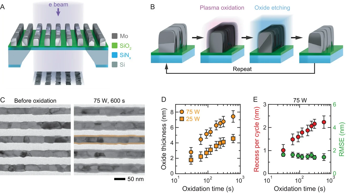
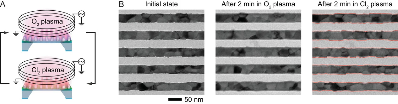
Molybdenum (Mo) has a high potential of becoming the material of choice for sub-10 nm scale metal structures in future integrated circuits (ICs). Manufacturing at this scale requires exceptional precision and consistency, so many metal processing techniques must be reconsidered. In particular, present direct wet chemical etching methods produce anisotropic etching profiles with significant surface roughness, which can be detrimental to device performance. Here, it is shown that polycrystalline Mo nanowires can be etched uniformly using a cyclic two-step “digital” method: the metal surface is first oxidized with isotropic oxygen plasma to form a layer of MoO3, which is then selectively removed using either wet chemical or dry isotropic plasma etching. These two steps are repeated in cycles until the intended metal recess is achieved. High uniformity of plasma oxidation defines the etching uniformity, and small metal recess per cycle (typically 1–2 nm) provides precise control over the etching depth. This method can replace wet etching where high etching precision is needed, enabling the reliable manufacturing of nanoscale metal interconnects.
Figures and videos: Erofeev et al., Adv Materials Inter 2024, CC BY 4.0
P09
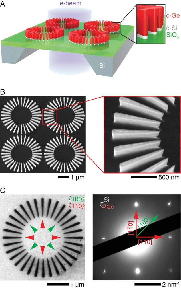
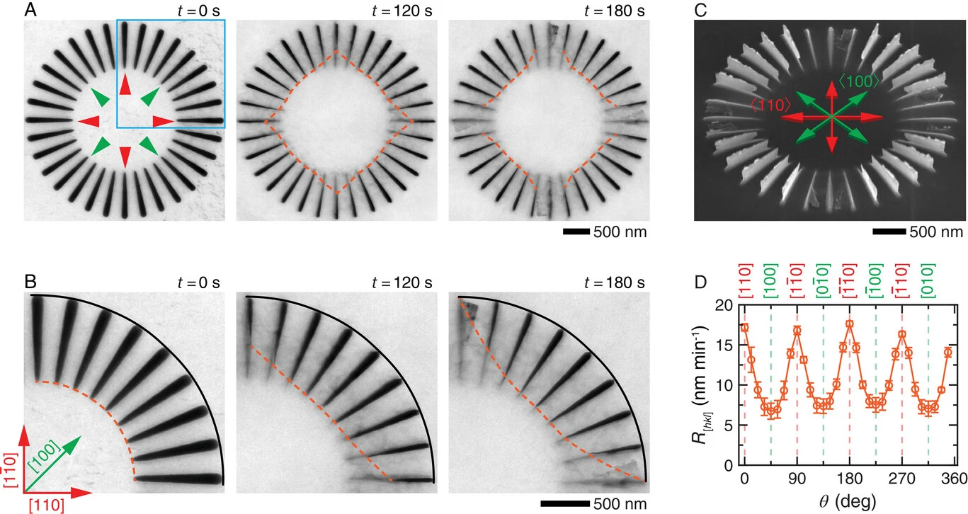
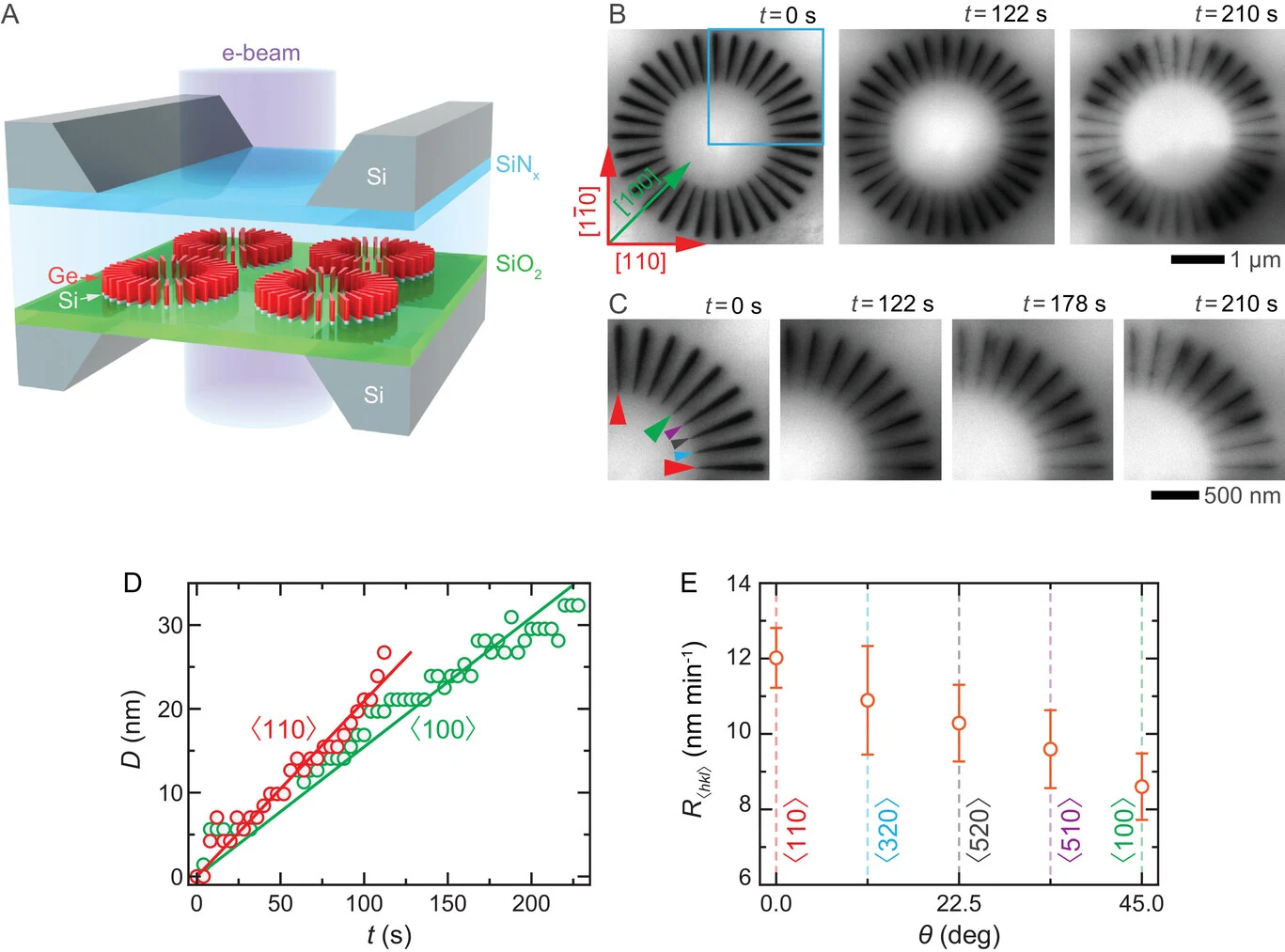
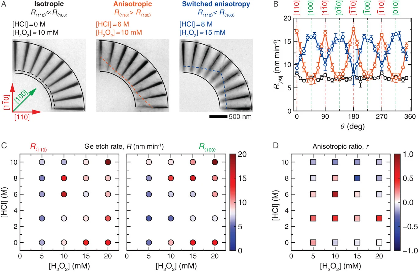
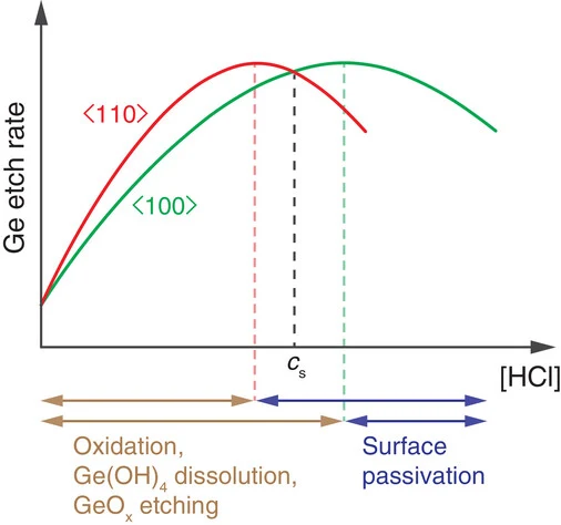
Orientation-dependent wet chemical etching of crystalline germanium (c-Ge) is essential for the fabrication of next-generation complementary metal oxide semiconductor (CMOS) devices. Here, using a combination of conventional and in situ liquid-phase transmission electron microscopy (TEM) imaging, we reveal the details of the wet etching process of c-Ge nanostructures and identify critical parameters that control the etching rates along different crystalline directions. We demonstrate that etching behavior can be changed from isotropic to anisotropic etching (i.e., from crystal-orientation-independent to orientation-dependent etching) by introducing hydrochloric acid (HCl) into a commonly used hydrogen peroxide (H2O2) etchant. The observations reveal that the relative etching rates along different crystal directions can be tuned by adjusting the HCl concentration, allowing for full control over the etch anisotropy. The study provides important insights into the nanoscale details of the wet etching of c-Ge and presents a new level of control required for the fabrication of advanced nanoelectronic devices.
Figures and videos: Saidov et al., Small 2025, CC BY-NC 4.0
New
Abstract of the paper.
Credit line (e.g. Reprinted with permission from …)
Read the paper03 / Lab Automation
I am developing an integrated approach to automate materials characterization across the experimental pipeline, spanning automated microscopy experiments, AI-driven data analysis, and structured data management.
The broader goal is to automate the materials characterization workflow from experiment to analysis, data management, and reporting, enabling more reproducible and scalable research.

01 Experiment
Thermo Fisher AutoScriptI develop automated microscopy workflows using Thermo Fisher AutoScript for FIB and TEM, enabling scripted instrument control, automated acquisition, and repeatable experimental sequences.
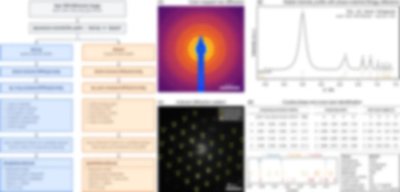
02 Analysis
Our team is developing AI-driven analysis workflows to extract quantitative information from microscopy and experimental data, enabling automated analysis of microstructure, morphology, and material evolution.

03 Data
eLabFTWOur team is developing eLabFTW-based workflows to organize experimental data, analysis results, metadata, and reporting, bringing different stages of the characterization process into a connected workflow.
04 / Publications
My publications reflect a broad research journey spanning nanoscale materials, nanofabrication, thermoelectrics, interfacial phenomena, and semiconductor processing, with advanced electron microscopy and AI analytics playing a central role in my research. With 94 publications, my work has evolved from materials characterization to understanding materials processes at increasingly smaller length and time scales. I have also reviewed 28+ manuscripts for international scientific journals.
| Google Scholar | OpenAlex | |
|---|---|---|
| Citations | 1,804 | 1,521 |
| h-index | 22 | 20 |
| i10-index | 47 | 38 |
| 2025 | Tuning catalyst-support interactions enable steering of electrochemical CO 2 reduction pathways M. Wang, Y. Li, J. Jia, T. Ghosh, P. Luo, Y. J. Shen, S. Wang, J. Zhang, S. Xi, Z. Mi, M. Zhang, W. R. Leow, B. Johannessen, Z. Aabdin, S. F. Hung, J. Zhang, Y. Lum Science Advances, 11 (14), eado5000 | 24 | 13.2 |
| 2024 | Controlled Stepwise Wet Etching of Polycrystalline Mo Nanowires K. Saidov, I. Erofeev, Z. Aabdin, A. Pacco, H. Philipsen, A. W. Hartanto, Y. Chen, H. Yan, W. W. Tjiu, F. Holsteyns, U. Mirsaidov Advanced Functional Materials, 34 (12), 2310838 | 21 | 15.7 |
| 2023 | Oxygen Plasma Induced Nanochannels for Creating Bimetallic Hollow Nanocrystals W. Y. Wu, S. Wu, W. W. Tjiu, H. R. Tan, F. Y. Leong, P. C. Lim, S. Wang, W. Jiang, R. Ji, Q. Zhu, M. Bosman, Q. Yan, Z. Aabdin ACS Nano, 17 (17), 17536–17544 | 5 | 18.2 |
| 2022 | Controlling the Wet-Etch Directionality in Nanostructured Silicon Z. Aabdin, T. Ghosh, A. Pacco, S. Raj, H. T. B. Do, K. Saidov, T. W. Weei, U. Anand, P. Král, F. Holsteyns, M. Bosman, U. Mirsaidov ACS Applied Electronic Materials, 4 (11), 5191–5198 | 15 | 5.2 |
| 2021 | Dynamics of thin precursor film in wetting of nanopatterned surfaces U. Anand, T. Ghosh, Z. Aabdin, S. Koneti, X. Xu, F. Holsteyns, U. Mirsaidov Proceedings of the National Academy of Sciences, 118 (38), e2108074118 | 26 | 8.8 |
| 2017 | Transient Clustering of Reaction Intermediates during Wet Etching of Silicon Nanostructures Z. Aabdin, X. M. Xu, S. Sen, U. Anand, P. Král, F. Holsteyns, U. Mirsaidov Nano Letters, 17 (5), 2953–2958 | 42 | 9.3 |
| 2014 | Bonding Pathways of Gold Nanocrystals in Solution Z. Aabdin, J. Lu, X. Zhu, U. Anand, N. D. Loh, H. Su, U. Mirsaidov Nano Letters, 14 (11), 6639–6643 | 95 | 9.3 |
Click a column to sort · Citations update weekly · *IF: journal 2-year mean citedness (OpenAlex), comparable to the Journal Impact Factor
Edit Publications05 / Patents
My research has resulted in patented technologies covering controlled nanoscale processing and analytical instrumentation, translating research concepts into practical tools and techniques.
2Patents
8Technology disclosures
| 2025 | Spectroscopy system for blood and/or tissue monitoring | SG Provisional Patent |
| 2022 | System and method for controlling directionality of fast-wet etching of crystalline silicon, c-Si U. Mirsaidov, M. Bosman, T. Ghosh, Z. Aabdin, F. Holsteyns, A. Pacco | Granted US Patent 11906946 |
| 2024 | High-precision terahertz spectroscopy system for non-invasive skin penetration and blood flow detection | IMRE TD |
| 2023 | Design and construction of single-tilt TEM holder suitable for EDX and EELS measurements of odd size samples | IMRE and NUS joint TD |
| 2023 | A system and method for evaluating coating layer quality on CFRP substrate | IMRE TD |
| 2022 | Modular smart DIP coating package | IMRE TD |
| 2021 | Digital Micrograph scripts for recording and processing TEM, STEM and EELS data | IMRE TD |
| 2021 | A TEM liquid-cell fabrication process optimized for industrial wafers | IMRE TD |
| 2019 | Chemically resistant liquid flow holder for transmission electron microscopes | IMRE and NUS joint TD |
06 / Grants
I have led two research projects supported by approximately S$1.4M in competitive research funding, including a National Research Foundation (NRF) Competitive Research Programme (CRP) grant and a Career Development Award (CDA).
Total
S$1.4M
Competitive research funding
2020 · 3 years · PI
S$600K
Career Development Award (CDA), A*STAR, Singapore
2021 · 4 years · Co-PI
S$786K
National Research Foundation (NRF) Competitive Research Programme (CRP), Singapore
07 / About
I am a Senior Scientist at the Institute of Materials Research and Engineering (IMRE), A*STAR, Singapore. I obtained my PhD in Applied Physics from the University of Tübingen, Germany, where I worked on the structural characterization of nanostructured superconducting and thermoelectric materials.
My research has developed around a simple question: how can we directly observe materials as they change? This led me toward advanced electron microscopy and, in particular, in-situ TEM, where materials can be studied while they react, transform, grow, or degrade.
Today, my work combines materials science with microscopy, computation, instrumentation, and automation. Alongside developing microscopy-based experiments, I build custom experimental hardware and software, develop AI-assisted image-analysis methods, and automate parts of the experimental workflow.
I have contributed to 94 research publications and patented technologies, and have led research projects supported by S$1.4M in competitive research funding. My broader interest is in developing experimental approaches that make nanoscale materials science more observable, quantitative, and reproducible.
08 / Contact
Interested in discussing research ideas, potential collaborations, or opportunities to work together? I welcome enquiries from researchers and industry partners.
Get in touch.
09 / Office
Institute of Materials Research and Engineering (IMRE), A*STAR
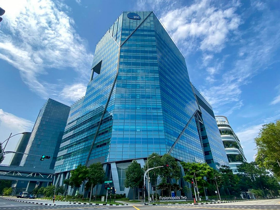
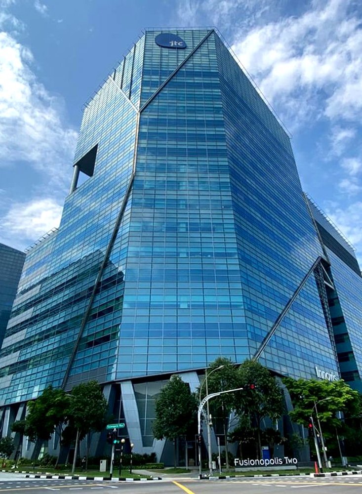
Fusionopolis Two, 2 Fusionopolis Way, Singapore 138634
One-north MRT
CC23 · Circle Line · 2 min walk
Opp One-North Stn (18059)
Ayer Rajah Ave · Bus 91 · 2 min walk